Chipmakers Embrace Advanced EUV Technology for Next-Gen Processors
ByKim Swift
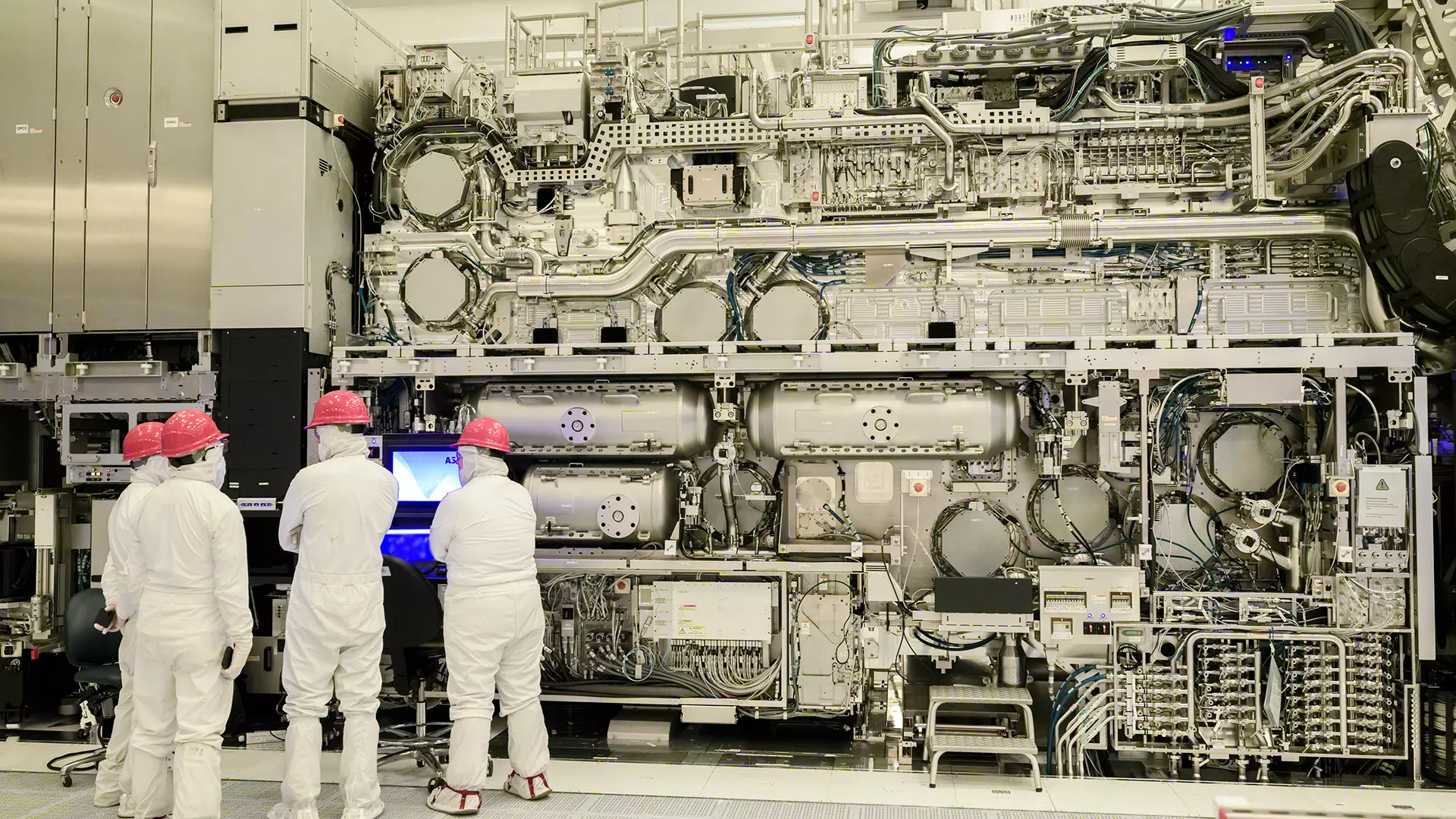
The semiconductor industry is on the cusp of a significant transformation, with leading chipmakers like Samsung and TSMC committing to ASML's groundbreaking High Numerical Aperture Extreme Ultraviolet (High NA EUV) lithography technology. This advanced manufacturing process is poised to revolutionize chip production, enabling the creation of smaller, faster, and more energy-efficient processors to meet the escalating demands of the artificial intelligence sector and other high-growth areas.
Alongside the adoption of High NA EUV, a collaborative effort is underway involving key industry players such as Samsung, TSMC, Nvidia, and Apple, aimed at transitioning from the current 6-inch photomasks to larger 12-inch formats. This strategic shift is expected to further streamline the manufacturing process, reduce production costs, and enhance overall efficiency, solidifying the industry's confidence in future market growth.
The Dawn of High NA EUV and Enhanced Chip Manufacturing
Major semiconductor firms, including Samsung and TSMC, are slated to integrate ASML's cutting-edge High NA EUV machines into their production lines by 2028 and 2030, respectively. This represents a significant leap forward in chip fabrication, promising superior chip density, accelerated production cycles, and a reduction in the number of manufacturing steps. Intel and SK Hynix have already begun utilizing aspects of this technology, paving the way for widespread adoption. The intrinsic advantages of High NA EUV, such as simplified processes and increased wafer density, are critical for overcoming current manufacturing bottlenecks and addressing the growing need for high-performance computing components.
The transition to High NA EUV signifies a pivotal moment for the semiconductor industry, as it will allow for the mass production of next-generation chips with unprecedented levels of precision and efficiency. This technology, characterized by its high numerical aperture, leverages extreme ultraviolet light to imprint intricate circuit patterns onto silicon wafers. By doing so, it facilitates the creation of microchips that are not only more powerful but also consume less energy, which is essential for the advancement of AI, data centers, and other computationally intensive applications. This widespread embrace of High NA EUV reflects a strong industry commitment to innovation and future-proofing production capabilities.
Transformative Potential of 12-inch Photomasks
In parallel with the adoption of High NA EUV, the semiconductor industry is embarking on a collaborative initiative to transition from 6-inch to 12-inch photomasks. These masks are crucial components in the lithography process, acting as stencils through which EUV light etches chip designs onto wafers. By increasing the size of these photomasks, a larger area of the wafer can be covered with each exposure, thereby reducing the number of individual shots required and minimizing the need for complex alignment processes. This innovation is projected to yield substantial improvements in manufacturing efficiency and cost-effectiveness, with a pilot line for 12-inch masks expected by 2031 and full integration into advanced node production by 2033.
This move towards larger photomasks, championed by ASML in cooperation with industry giants like Samsung, TSMC, Nvidia, and Apple, is a testament to the continuous drive for optimization within chip manufacturing. The benefits extend beyond mere scale, encompassing enhanced throughput, reduced defects, and ultimately, lower unit costs for advanced chips. The strategic timing of these technological advancements, occurring against the backdrop of an insatiable demand for AI-driven hardware, underscores the industry's proactive approach to meeting market needs. The synergy between High NA EUV and 12-inch photomasks promises to usher in an era of unprecedented semiconductor performance and accessibility, ensuring that the foundational components for future technological innovations are readily available.
About the author
Kim Swift
Video game designer known for pioneering work on "Portal," focusing on innovative puzzle mechanics.